We have compiled a list of manufacturers, distributors, product information, reference prices, and rankings for Flip Chip Bonder.
ipros is IPROS GMS ・ IPROS One of the largest technical database sites in Japan that collects information on.

Flip Chip Bonder Product List and Ranking from 7 Manufacturers, Suppliers and Companies | IPROS GMS

Last Updated: Aggregation Period:Sep 02, 2026~Sep 29, 2026
This ranking is based on the number of page views on our site.

Flip Chip Bonder Manufacturer, Suppliers and Company Rankings

Last Updated: Aggregation Period:Sep 02, 2026~Sep 29, 2026
This ranking is based on the number of page views on our site.

  1. テクノアルファ Tokyo//Electronic Components and Semiconductors
  2. 澁谷工業 Ishikawa//Other manufacturing
  3. null/null
  4. 4 Ito Corporation Tokyo//Electronic Components and Semiconductors
  5. 5 ハイソル Tokyo//Electronic Components and Semiconductors

Flip Chip Bonder Product ranking

Last Updated: Aggregation Period:Sep 02, 2026~Sep 29, 2026
This ranking is based on the number of page views on our site.

  1. Tabletop Semi-Automatic Die Bonder Flip Chip Bonder テクノアルファ
  2. High-precision multi-die bonder flip chip bonder テクノアルファ
  3. High-precision die bonder / flip chip bonder FDB210 / 211 澁谷工業
  4. 4 High-precision die bonder and flip chip bonder 'lambda2'
  5. 4 Small-scale production and development die bonder / flip chip bonder DB258 澁谷工業

Flip Chip Bonder Product List

1~12 item / All 12 items

Displayed results

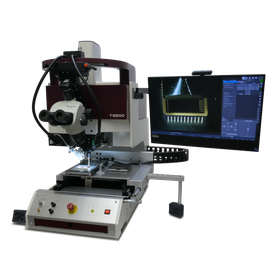
High-precision multi-die bonder flip chip bonder

Supports the installation of multi-functional high-precision components! Compatible with applications requiring advanced load control and image recognition. [Demo units available for loan]

The "FALCON Series" is a die flip chip die bonder that offers a lineup of devices tailored to user needs, ranging from manual to automatic specifications. We can manufacture die flip chip bonders according to your company's required specifications by combining various options. We can propose devices suitable for your specifications, including heating mechanisms, high-load bonding, wafer pickup, and chip flipping functions. Additionally, there are higher models that can accommodate fully automatic specifications with attachments like conveyors, and since these are our own products, we can flexibly respond to your desired customization specifications. 【Features】 ■ Operability Achieves smooth XY stage operability using a joystick. Basic operations can be completed easily with the joystick, providing simple operation specifications. ■ Load Control Supports applications requiring advanced load control through program operation by a motor (Z-axis resolution in micrometers) and VCM control (optional). ■ Software User interface design that does not require a manual. User-friendly specifications that allow for easy setting of bonding parameters and recognition program creation. *For more details, please download the PDF materials.

  • IPROS14832388318700197206.jpg
  • ?.jpg
  • ?.JPG
  • ?.JPG
  • ?.JPG
  • X操作性.PNG
  • 荷重制御.PNG
  • ソフトウェア.PNG
  • 画像認識.PNG
  • Bonding Equipment
  • Flip Chip Bonder

Added to bookmarks

Bookmarks list

Bookmark has been removed

Bookmarks list

You can't add any more bookmarks

By registering as a member, you can increase the number of bookmarks you can save and organize them with labels.

Free membership registration

Flip Chip Bonder "FB2000SS"

Supports various processes with head exchange! Achieves a wide dynamic range through a low-friction pressurization mechanism.

The "FB2000SS" is a flip chip bonder suitable for high-precision semiconductor mounting. The ultrasonic horn is directly clamped by a rigid clamp. High rigidity clamping ensures high flatness even under high loads. Additionally, it features an alignment calibration function that corrects for temporal changes, along with dual-field recognition, achieving stable high-precision mounting. 【Features】 ■ High-rigidity horn clamp mechanism ■ High-precision alignment ■ High-function position load control ■ Compatible with various processes through head exchange *For more details, please download the PDF or feel free to contact us.

  • Other processing machines
  • Flip Chip Bonder

Added to bookmarks

Bookmarks list

Bookmark has been removed

Bookmarks list

You can't add any more bookmarks

By registering as a member, you can increase the number of bookmarks you can save and organize them with labels.

Free membership registration

Small-scale production and development die bonder / flip chip bonder DB258

The flip chip bonder is ideal for small-scale production and development, perfect for high-precision assembly required for optical devices and more.

This machine is a high-precision semi-automatic flip chip bonder suitable for experiments, development, and small-scale production. With a digitally adjustable pulse heat stage and various options, it can handle a wide range of assembly processes with just this one unit.

  • Bonding Equipment
  • Flip Chip Bonder

Added to bookmarks

Bookmarks list

Bookmark has been removed

Bookmarks list

You can't add any more bookmarks

By registering as a member, you can increase the number of bookmarks you can save and organize them with labels.

Free membership registration

High-precision die bonder / flip chip bonder FDB210 / 211

It is a high-precision die bonder optimized for mass production of optical devices. Additionally, we also offer the highly precise FDB210P in our lineup.

This machine is a high-precision bonder for the production of optical communication modules/optical devices suitable for mass production. It also supports flip-chip and mounting. There are two types: the FDB210 model, which supplies chips and substrates via trays, and the FDB211 model, which supplies with grip rings.

  • Other semiconductor manufacturing equipment
  • Flip Chip Bonder

Added to bookmarks

Bookmarks list

Bookmark has been removed

Bookmarks list

You can't add any more bookmarks

By registering as a member, you can increase the number of bookmarks you can save and organize them with labels.

Free membership registration

Flip chip bonder, high-precision die bonder

Ideal for prototype development of laser diodes and fine chip implementation.

Installation of two cameras, top and bottom. Alignment based on chip alignment marks, bumps, pads, and outlines. High-precision bonding is performed. A general-purpose simple flip chip bonder that is not restricted by device types, materials, or bonding methods.

  • Steel
  • Flip Chip Bonder

Added to bookmarks

Bookmarks list

Bookmark has been removed

Bookmarks list

You can't add any more bookmarks

By registering as a member, you can increase the number of bookmarks you can save and organize them with labels.

Free membership registration

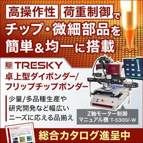
Tabletop Semi-Automatic Die Bonder Flip Chip Bonder

Ideal for small-batch, multi-variety production and research and development! With simple operability, it is easy to mount chips and fine components. *Comprehensive catalog available.

Swiss company Dr. Tresky has been developing, manufacturing, and selling various assembly equipment since its establishment in Switzerland in 1980. We offer a lineup ranging from simple fully manual machines with excellent scalability to semi-automatic machines, and we have a wide range of delivery records from low-volume, high-variety production to research and development sites. 【Features of T-5300/T-5300-W】 ■ When mounting chips, regardless of changes in chip thickness, they can always be mounted parallel to the substrate with the set load. ■ Wide work table (250×330mm). ■ With optional combinations, the device configuration can be tailored for specifications such as die bonding and flip chip bonding. ■ Additional options can be retrofitted. ■ When using optional heaters or ultrasonic units, parameters such as heater warm-up timing (simultaneous start with load detection, cooling timing settings), ultrasonic emission timing, Z-axis mounting time, and rise timing can be set arbitrarily. ■ When using the optional beam splitter camera, accuracy of up to ±1μ can be achieved. *For more details, please download the PDF or feel free to contact us.

  • IPROS31278937468233384034.png
  • T-4909-AE?.png
  • IPROS90074725736833130928.png
  • tresky_14.png
  • TRESKY広告画像.jpeg
  • Bonding Equipment
  • Flip Chip Bonder

Added to bookmarks

Bookmarks list

Bookmark has been removed

Bookmarks list

You can't add any more bookmarks

By registering as a member, you can increase the number of bookmarks you can save and organize them with labels.

Free membership registration

3D Semiconductor Research Center Business Introduction

We provide a semiconductor development environment tailored to meet utilization needs!

The Fukuoka Prefectural Industrial and Scientific Technology Promotion Foundation's 3D Semiconductor Research Center is a facility equipped with implementation and evaluation equipment necessary to support research and development, prototyping, and evaluation for stacking multiple semiconductor chips in three dimensions to achieve high density in semiconductor-related products. With approximately 80 types of rental equipment available, we support the creation of new added value by combining each user's development themes with the foundational technologies of our center. 【Business Activities】 ○ Support for semiconductor design, implementation, prototyping, demonstration experiments, and evaluation ○ Provision of semiconductor development environments tailored to user needs For more details, please contact us or download the catalog.

Added to bookmarks

Bookmarks list

Bookmark has been removed

Bookmarks list

You can't add any more bookmarks

By registering as a member, you can increase the number of bookmarks you can save and organize them with labels.

Free membership registration

ASMPT manufactured flip chip bonder/die bonder AFCPlus

AFC Plus is a flip chip bonder capable of bonding dies to wafers/substrates/dies with high precision.

"AFC Plus" is a device that enables bonding of high-precision, diced chips to wafers/substrates/dies using the company's patented alignment technology. 【Features】 - Alignment accuracy: ±1µm @ 3s - Alignment technology (patented) - Bonding methods during the joining process - Extensive track record in optical communication and silicon photonics - Rich experience in MEMS sensors, LiDAR, VCSEL, etc. - Extensive experience in R&D and mass production facilities 【Main Specifications】 - Alignment accuracy: ±0.2µ@3σ - Cycle time: 20 to 30 sec (varies by material) - Die size: 0.1mm to 20mm - Substrate size: MAX 300 x 300 mm - Bonding force (load): 10g to 2kg - Joining methods: eutectic solder, epoxy, UV-curable resin, laser bonding *Ultrasonic bonding is not supported.

  • Bonding Equipment
  • Flip Chip Bonder

Added to bookmarks

Bookmarks list

Bookmark has been removed

Bookmarks list

You can't add any more bookmarks

By registering as a member, you can increase the number of bookmarks you can save and organize them with labels.

Free membership registration